AIM:
Design a Half and Full Adder
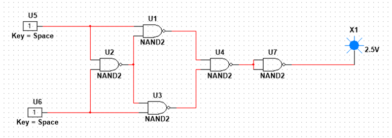
Truth Table of Half Adder
| Inputs | Outputs | ||
| A | B | S (Sum) | C (Carry) |
| 0 | 0 | 0 | 0 |
| 0 | 1 | 1 | 0 |
| 1 | 0 | 1 | 0 |
| 1 | 1 | 0 | 1 |
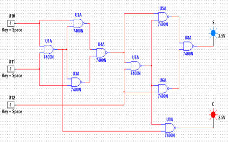
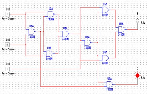
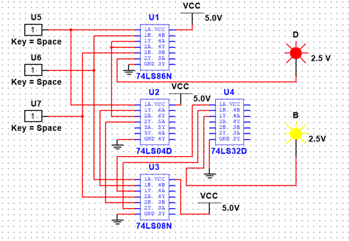
Circuit Diagram:
Truth Table of Full Adder
| Inputs | Outputs | |||
| X | Y | Z | S (Sum) | C(Carry) |
| 0 | 0 | 0 | 0 | 0 |
| 0 | 0 | 1 | 1 | 0 |
| 0 | 1 | 0 | 1 | 0 |
| 0 | 1 | 1 | 0 | 1 |
| 1 | 0 | 0 | 1 | 0 |
| 1 | 0 | 1 | 0 | 1 |
| 1 | 1 | 0 | 0 | 1 |
| 1 | 1 | 1 | 1 | 1 |
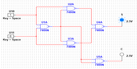
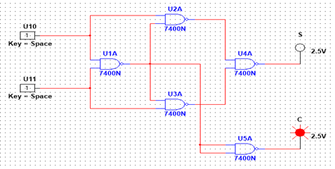
Circuit Diagram: