INTRODUCTION:
8085 is an 8-bit microprocessor as it operates on 8 bits at a time. It is a 40-pin dual-in-line chip.

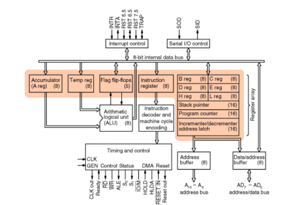
Control Unit: Generates signals within microprocessor to carry out the instruction, which has been decoded. In reality causes certain connections between blocks of the microprocessor to be opened or closed, so that data goes where it is required, and so that ALU operations occur.
Arithmetic Logic Unit: The ALU performs the actual numerical and logic operation such as ‘add’, ‘subtract’, ‘AND’, ‘OR’, etc. Uses data from memory and from Accumulator to perform arithmetic. Always stores result of operation in Accumulator.
Registers: The 8085/8080A-programming model includes six registers, one accumulator, and one flag register, as shown in Figure. In addition, it has two 16-bit registers: the stack pointer and the program counter. They are described briefly as follows. The 8085/8080A has six general-purpose registers to store 8-bit data; these are identified as B, C, D, E, H, and L as shown in the figure. They can be combined as register pairs – BC, DE, and HL – to perform some 16-bit operations. These pairs are referred to as the extended registers. The programmer can use these registers to store or copy data into the registers by using data copy instructions.
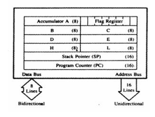
Accumulator: The accumulator is an 8-bit register that is a part of arithmetic/logic unit (ALU). This register is used to store 8-bit data and to perform arithmetic and logical operations. The result of an operation is stored in the accumulator. The accumulator is also identified as register A.
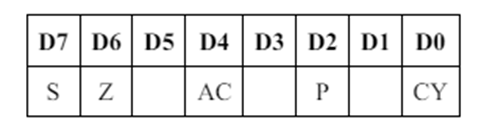
Flags: The ALU includes five flip-flops, which are set or reset after an operation according to data conditions of the result in the accumulator and other registers. They are called Zero(Z), Carry (CY), Sign (S), Parity (P), and Auxiliary Carry (AC) flags; they are listed in the Table and their bit positions in the flag register are shown in the Figure below. The most commonly used flags are Zero, Carry, and Sign. The microprocessor uses these flags to test data conditions. For example, after an addition of two numbers, if the sum in the accumulator id larger than eight bits, the flip-flop uses to indicate a carry – – called the Carry flag (CY) – is set to one. When an arithmetic operation results in zero, the flip-flop called the Zero(Z) flag is set to one. The first Figure shows an 8-bit register, called the flag register, adjacent to the accumulator. However, it is not used as a register; five bit positions out of eight are used to store the outputs of the five flip-flops. The flags are stored in the 8-bit register so that the programmer can examine these flags (data conditions) by accessing the register through an instruction These flags have critical importance in the decision-making process of the microprocessor. The conditions (set or reset) of the flags are tested through the software instructions. For example, the instruction JC (Jump on Carry) is implemented to change the sequence of a program when CY flag is set. The thorough understanding of flag is essential in writing assembly language programs.
Program Counter (PC): This 16-bit register deals with sequencing the execution of instructions. This register is a memory pointer. Memory locations have 16-bit addresses, and that is why this is a 16-bit register. The microprocessor uses this register to sequence the execution of the instructions. The function of the program counter is to point to the memory address from which the next byte is to be fetched. When a byte (machine code) is being fetched, the program counter is incremented by one to point to the next memory location.
Stack Pointer (SP): The stack pointer is also a 16-bit register used as a memory pointer. It points to a memory location in R/W memory, called the stack. The beginning of the stack is defined by loading 16-bit address in the stack pointer.
Instruction Register/Decoder: Temporary store for the current instruction of a program. Latest instruction sent here from memory prior to execution. Decoder then takes instruction and ‘decodes’ or interprets the instruction. Decoded instruction then passed to next stage. Memory Address Register Holds address, received from PC, of next program instruction. Feeds the address bus with addresses of location of the program under execution.
Control Generator: Generates signals within microprocessor to carry out the instruction which has been decoded. In reality causes certain connections between blocks of the microprocessor to be opened or closed, so that data goes where it is required, and so that ALU operations occur
Introduction to Programming with 8085:
These concepts are fundamental to understanding and programming the 8085-microprocessor efficiently.
Data Transfer Operations:
1. MOV – Move Data: Hex Mnemonic: 8-bit transfer: MOV A, B – 78, this instruction will copy the contents of “B” to “A”
2. MVI – Move Immediate: Hex Mnemonic: MVI A, 45H – 3E 45
3. LXI – Load Register Pair Immediate: Hex Mnemonic: LXI B, 2032H – 01 32 20
4. LDA – Load Accumulator Direct: Hex Mnemonic: LDA 3000H – 3A 00 30
5. STA – Store Accumulator Direct: Hex Mnemonic: STA 3000H – 32 00 30
Arithmetic Operations:
1. ADD – Add: Hex Mnemonic: ADD B – 80
2. ADC – Add with Carry: Hex Mnemonic: ADC C – 89
3. SUB – Subtract: Hex Mnemonic: SUB M – 96
4. SBB – Subtract with Borrow: Hex Mnemonic: SBB A – 9F
5. INR – Increment Register: Hex Mnemonic: INR D – 14
6. DCR – Decrement Register: Hex Mnemonic: DCR E – 1D
Logical Operations:
1. ANA – Logical AND: Hex Mnemonic: ANA B – A0
2. ORA – Logical OR: Hex Mnemonic: ORA C – B1
3. XRA – Logical XOR: Hex Mnemonic: XRA D – A2
4. CMP – Compare: Hex Mnemonic: CMP E – BA
5. CMA – Complement Accumulator: Hex Mnemonic: CMA – 2F
Control Transfer Operations:
1. JMP – Jump: Hex Mnemonic: JMP 3000H – C3 00 30
2. CALL – Call Subroutine: Hex Mnemonic: CALL 4000H – CD 00 40
3. RET – Return: Hex Mnemonic: RET – C9
4. RST – Restart: Hex Mnemonic: RST 5 – E7
Stack Operations:
1. PUSH – Push Data onto Stack: Hex Mnemonic: PUSH H – E5
2. POP – Pop Data from Stack: Hex Mnemonic: POP D – D1
These are some of the key operations in the 8085-microprocessor along with their corresponding hexadecimal mnemonics.
Sample program:
| Memory | Instruction | Hex pneumonic |
| 2000 | MVI, A | |
| 2001 | 09 | 09 |
| 2002 | MVI B | |
| 2003 | 11 | 11 |
| 2004 | ADD B |
This program stores 09 (H) in A, 11 (H) in B then adds contents of B to A, which is equivalent of programming statement “A=A+B;”
8085 ADDRESSING MODES
The instructions MOV B, A or MVI A, 82H are to copy data from a source into a destination. In these instructions the source can be a register, an input port, or an 8-bit number (00H to FFH). Similarly, a destination can be a register or an output port. The sources and destination are operands. The various formats for specifying operands are called the ADDRESSING MODES. For 8085, they are:
- Immediate addressing: Operand is part of the instruction.
- Register addressing: Operand is stored in a register or register pair
- Direct addressing: Operand is stored in the memory and the memory address is specified with the instruction
- Indirect addressing: The memory address of the operand is stored in a register pair
- Implied: operand is not specified, yet it is implied
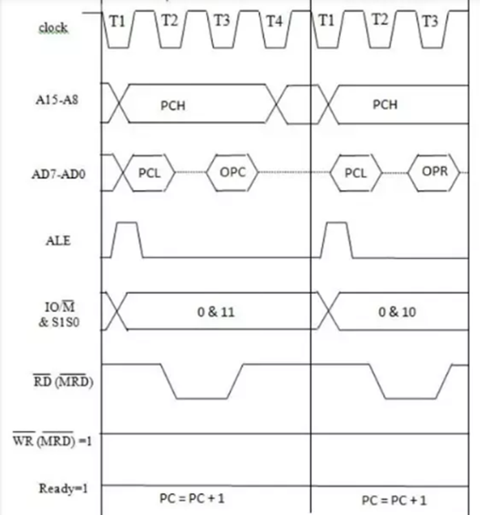
Timing diagram:
The timing diagram for the MVI B instruction in an 8-bit microprocessor typically consists of several distinct phases:
- Instruction Fetch: During this phase, the microprocessor fetches the MVI B instruction from memory. This involves sending out the address of the instruction to the memory and receiving the opcode for MVI B.
- Memory Read: In this phase, the microprocessor reads the data byte (the immediate data) from the memory location immediately following the opcode of the MVI B instruction.
- Instruction Execution: During this phase, the microprocessor executes the MVI B instruction by loading the immediate data into the B register. This phase involves transferring the data from the memory buffer to the B register
Opcode fetch Memory read