Metal Oxide Semiconductor Field Effect Transistor
Aim:
To study the V-I characteristics of MOSFET
Apparatus Required:
- MOSFET
- Bread board
- Resistor
- Two Voltage Sources
- Connecting Wires
Theory:
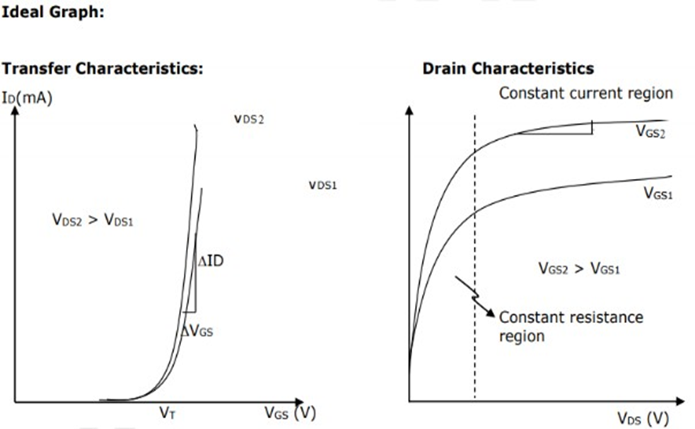
MOSFT stands for Metal Oxide Semiconductor Field Effect Transistor. It is actually a four terminal device whose substrate terminal must be always hold at one of the extreme voltage in the circuit either the most positive for PMOS or the most negative for NMOS. One unique property of MOSFET is that the gate drains no measurable current. The body of any N-channel MOSFET is made up of P-type material. 2 N-type materials are diffused at the top. A depletion region will be formed in the PN junction. A metal contact is made at the bottom of the P-type substrate and a terminal is taken out called the body or substrate. Similarly, a metal contact is made at the top of both the N-type materials, and two terminals are taken out as Drain and source. A Silicon dioxide layer is drawn in between the two N-type wells at the top. A metal contact is made at the top of it and a terminal is taken out called a Gate terminal. MOSFET is used as a high-frequency amplifier, brushless DC motor drives, electronic DC relays, inverter. The voltage at which the channel of the MOSFET closes is called the “pinch-off voltage”. When VDS is increased beyond the pinch-off voltage, VGS controls the channel current and VDS has little or no effect i.e. remains constant.
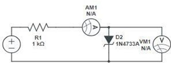
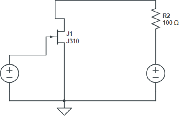
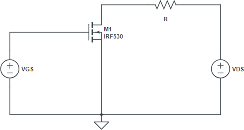
Circuit Diagram:
Procedure :
Output/Drain Characteristics
- Connect the circuit as per diagram properly
- Keep VGS constant at some value by varying VGG.
- Vary VDS and measure the drain current ID. Tabulate all the readings.
- Repeat the above procedure for VGS for different values
Transfer Characteristics
- Connect the circuit as per given diagram properly.
- Set the voltage VDS constant at a particular voltage.
- Vary VGS by varying VGG and note down value of drain current ID. Tabulate all the readings.
- Plot the output characteristics VDS versus ID and transfer characteristics VGS versus ID.
Observation:
Output/ Drain Characteristics
| VGS = | VGS = | VGS = | VGS = | VGS = | |||||
| VDS(V) | ID(mA) | VDS(V) | ID(mA) | VDS(V) | ID(mA) | VDS(V) | ID(mA) | VDS(V) | ID(mA) |
Transfer Characteristics
| VDS = | |
| VGS (V) | ID (mA) |
Result:
Hence, when we apply and vary VDS at constant VGS then ID increases and after some time it becomes constant.
Precaution:
- The reading should be in multiple of least count.
- For accuracy current should be taken in mA.