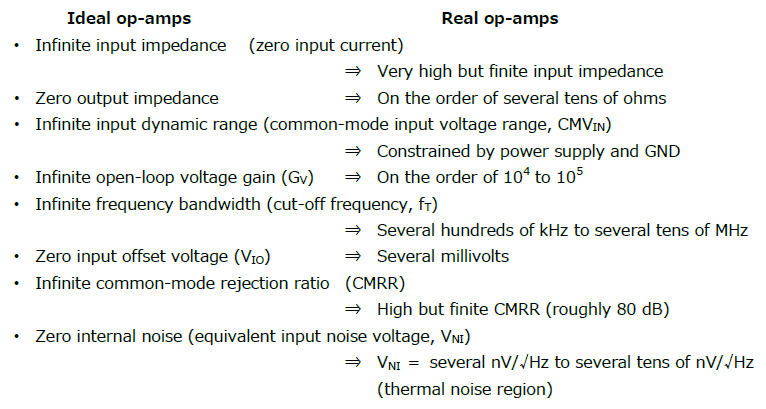
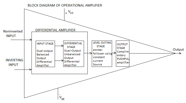
Op-amp block diagram
- Input Stage − The input stage is the dual input, balanced output differential amplifier. This stage provides most of the voltage gain and introduces the input resistance of the operational amplifier.
- Intermediate Stage − This stage is a dual input, unbalanced output differential amplifier, which is driven by the output of the first stage.
- Level Shifting Stage − Since direct coupling is used, therefore the DC voltage at the output of the intermediate stage is above the ground potential. Hence, the level shifting transistor circuit is used after the intermediate stage to shift the DC level at intermediate stage output downward to zero volts with respect to ground.
- Output Stage − The output stage is a push-pull complementary amplifier. The output stage increases the output voltage. The output stage also provides low output resistance.
Op-amp ic introduction and pin diagram
The pin configur ation of the IC 741 operational amplifier is shown below. The op amp 741 pin diagram and the functionality of each pin are explained clearly in the below section.
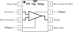
IC 741 Pin Diagram
Power Supply Pins: Pin 4 and 7
Pin 4 and pin 7 are the negative and positive voltage power supply terminals. The power which is required for the IC to function is received from both these pins. The voltage level between these pins can be in the range of 5 – 18V.
Output Pin: Pin 6
The output which is delivered from the IC 741 op amp is received from this pin. The output voltage that is received at this pin is based on the feedback approach that is used and the voltage level at the input pins.
When the voltage value at pin 6 is high, this corresponds to the output voltage being similar to the +ve supply voltage. In the same way, when the voltage value at pin 6 is low, this corresponds to the output voltage being similar to the -ve supply voltage.
Input Pins: Pin 2 and Pin 3
These are the input pins for the operational amplifier. Pin 3 is considered as the inverting input while pin 3 is considered as the non-inverting input pin. When the voltage value at pin 2 >> pin 3 which means that inverting input has a high value of voltage, then the output signal is low.
In the same way, when the voltage value at pin 3 >> pin 2 which means that non- inverting input has a high value of voltage, then the output signal is high.
Offset Null Pins: Pin 1 and Pin 5
As discussed before, this operational amplifier has an increased level of voltage gain. Because of this, even minimal variations in the voltages at both non-inverting and inverting inputs happen because of the abnormalities in the constructional procedure or other anomaly’s will show an impact on the output.
In order to overcome this, an offset value of the voltage to be applied at pin 1 and pin 5, and this generally accomplished by a potentiometer.
Not Connected Pin: Pin 8
It is just a pin that is used to fill up the empty pin in the IC 741 Op Amp. It has no connection with any of the internal or external circuits.
Specifications of IC 741 Op-Amp
The characteristics of the IC 741 operational amplifier include the following
- Power supply: For the functionality of this operational amplifier, it requires a minimum voltage of 5V and it can handle up to 18V.
- Input Impedance: It has a range of about 2 megaohms
- Output Impedance: It has a range of about 75 ohms
- Voltage gain: The voltage gain is 2,00,000 for a minimal range of frequencies
- Input offset range: This IC 741 Op Amp has an input offset range in between 2 – 6 mV
- Output Load: The recommended range is > 2 Kilo Ohms
- Slew Rate: This is defined as the maximum change in output voltage/unit of time. SR is measured in volts/µsec and represented as: SR = dVo/dt. For an IC 741 operational amplifier, the slew rate is 0.5V/microsec which is minimal.