Design a Half and Full Adder
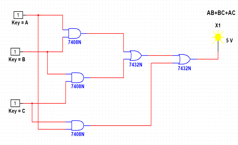
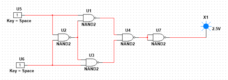
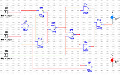
AIM: Design a Half and Full Adder Truth Table of Half Adder Inputs Outputs A B S (Sum) C (Carry) 0 0 0 0 0 1 1 0 1 0 1 0 1 1 0 1 Circuit Diagram: Truth Table of Full […]
Design a Half and Full Adder Read More »
DIGITAL ELECTRONICS